FPGA - Zero to Hero: Vol 3 #
In the previous blog I create a very basic code to toggle a PIN on a ALtera based FPGA board. I will continue my journey with the board and we will try to get a UART working on the board. There is RS232 IP available and Example provided by Altera for Quartus II and might not have changed much for Quartus Prime Lite but we are going to go the hard way and implement a bare metal UART (not production ready but a small test) for educational purpose only. We will also connect it to a Raspberry PI UART port to send and receive data between the two boards.
To create a UART TX and RX we need to understand how UART Works. UART is Universal Asynchronous Receiver/Transmitter (UART) is a popular hardware communication protocol used in serial communication. It enables the asynchronous transmission of data between devices without the need for a shared clock. So not sharing the clock makes it popular as dealing with clock like in some protocol like Serial Peripheral Interface (SPI more about in future blogs) is not easy from HW design perspective and also SPI needs >= 4 wires while UART only needs 2 wires.
Here is basic feature of a UART protocol: It has an UART Transmitter and an UART Receiver The protocol has a Start Bit and Stop bit Parity bit and Data bits. [UART Transmitter] — (TX) Start Bit, Data Bits, Parity, Stop Bit —> [UART Receiver]
UART Transmitter Code #
`timescale 1ns / 1ps

module uart_tx #(
    parameter CLOCK_FREQ = 50000000,
    parameter BAUD_RATE  = 115200
)(
    input clk,
    input rst,
    input [7:0] tx_data,
    input tx_start,
    output reg tx,
    output reg tx_busy
);

    localparam integer BAUD_COUNTER_MAX = CLOCK_FREQ / BAUD_RATE;
    localparam [2:0] IDLE  = 3'b000,
                     START = 3'b001,
                     DATA  = 3'b010,
                     STOP  = 3'b011;

    reg [2:0] state;
    reg [15:0] baud_cnt;
    reg [3:0] bit_index;
    reg [7:0] tx_shift;

    always @(posedge clk or posedge rst) begin
        if (rst) begin
            state     <= IDLE;
            tx        <= 1'b1;
            baud_cnt  <= 0;
            bit_index <= 0;
            tx_busy   <= 0;
        end else begin
            case (state)
                IDLE: begin
                    tx <= 1'b1;
                    baud_cnt <= 0;
                    bit_index <= 0;
                    tx_busy <= 0;
                    if (tx_start) begin
                        state    <= START;
                        tx_busy  <= 1;
                        tx_shift <= tx_data;
                    end
                end
                START: begin
                    tx <= 1'b0;
                    if (baud_cnt < BAUD_COUNTER_MAX-1)
                        baud_cnt <= baud_cnt + 1;
                    else begin
                        baud_cnt <= 0;
                        state    <= DATA;
                    end
                end
                DATA: begin
                    tx <= tx_shift[0];
                    if (baud_cnt < BAUD_COUNTER_MAX-1)
                        baud_cnt <= baud_cnt + 1;
                    else begin
                        baud_cnt  <= 0;
                        tx_shift  <= tx_shift >> 1;
                        bit_index <= bit_index + 1;
                        if (bit_index == 7)
                            state <= STOP;
                    end
                end
                STOP: begin
                    tx <= 1'b1;
                    if (baud_cnt < BAUD_COUNTER_MAX-1)
                        baud_cnt <= baud_cnt + 1;
                    else begin
                        baud_cnt <= 0;
                        state    <= IDLE;
                        tx_busy  <= 0;
                    end
                end
                default: state <= IDLE;
            endcase
        end
    end

endmodule
lets break down the code and try to understand the code piece-by-piece.
The first part is quite easy to understand. It is just a module template where we have CLOCK_FREQ of 50000000. and BAUD_RATE of 115200 bps with Ports as clk is the system clock, and rst is used to asynchronously reset the transmitter.tx_data carries the 8-bit data to be sent serially. tx_start triggers the start of the transmission.tx is the serial output. In UART, the idle state is high and tx_busy signals that the transmitter is active.
module uart_tx #(
    parameter CLOCK_FREQ = 50000000,
    parameter BAUD_RATE  = 115200
)(
    input clk,
    input rst,
    input [7:0] tx_data,
    input tx_start,
    output reg tx,
    output reg tx_busy
);
The state machine is the thing that need better explanation.
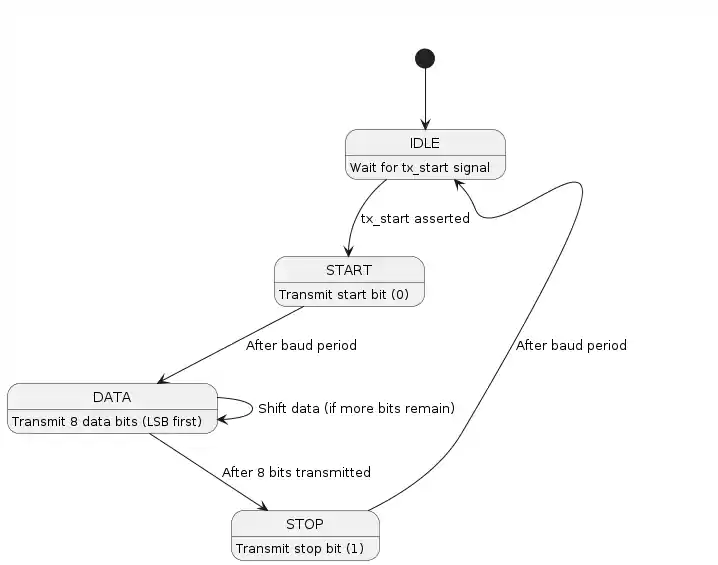
As I have explained in my previous blog Link verilog is a descriptive language that describes a hardware hence it is easy to build a sequential circuit. What we use in the design is something call memory elements to pass the pass output of a combinational circuit into next combinational block with help of clocks and memory elements. Flip Flops and Shift Registers are one type of memory elements that might be used.
So states being sequential must be implemented with memory.In verilog this can be done using always @(posedge clk) begin ... end block. This
Lets start with IDLE state.The UART line tx stays high. All counters are reset.tx_busy is set low. When tx_start is asserted, the module loads the 8-bit tx_data into the shift register and transitions to the START state.We also set tx_busy high to indicate an ongoing transmission.
    IDLE: begin
        tx <= 1'b1;
        baud_cnt <= 0;
        bit_index <= 0;
        tx_busy <= 0;
        if (tx_start) begin
            state <= START;
            tx_busy <= 1;
            tx_shift <= tx_data;
        end
    end
In START state he start bit is driven low on the tx line.The baud_cnt counts clock cycles until a complete bit count period is reached.After one bit period, the state moves to DATA.
    START: begin
        tx <= 1'b0;
        if (baud_cnt < BAUD_COUNTER_MAX-1)
            baud_cnt <= baud_cnt + 1;
        else begin
            baud_cnt <= 0;
            state <= DATA;
        end
    end
In DATA state The lowest significant bit of tx_shift is sent out first. The bit is heald for timing calculated by baud counter. After the bit period, the data is shifted right so that the next bit becomes the LSB.The bit_index is incremented. Once 8 bits are transmitted (when bit_index reaches 7), the state machine advances to the STOP state.
    DATA: begin
        tx <= tx_shift[0];
        if (baud_cnt < BAUD_COUNTER_MAX-1)
            baud_cnt <= baud_cnt + 1;
        else begin
            baud_cnt  <= 0;
            tx_shift  <= tx_shift >> 1;
            bit_index <= bit_index + 1;
            if (bit_index == 7)
                state <= STOP;
        end
    end
In STOP the stop bit which is logic high is transmitted.The baud counter again ensures that the stop bit is held for one full bit period.Once completed, the state machine returns to the IDLE state, and tx_busy is cleared.
                STOP: begin
                    tx <= 1'b1;
                    if (baud_cnt < BAUD_COUNTER_MAX-1)
                        baud_cnt <= baud_cnt + 1;
                    else begin
                        baud_cnt <= 0;
                        state    <= IDLE;
                        tx_busy  <= 0;
                    end
                end
                default: state <= IDLE;
To test the code we need to write a testbench. I have written a small test bench with the test cases:
`timescale 1ns / 1ps

module uart_tx_tb;
    reg clk;
    reg rst;
    reg [7:0] tx_data;
    reg tx_start;

    // Outputs
    wire tx;
    wire tx_busy;

    // Clock
    parameter CLOCK_FREQ = 50000000;
    parameter BAUD_RATE  = 9600;

    uart_tx #(
        .CLOCK_FREQ(CLOCK_FREQ),
        .BAUD_RATE(BAUD_RATE)
    ) uut (
        .clk(clk),
        .rst(rst),
        .tx_data(tx_data),
        .tx_start(tx_start),
        .tx(tx),
        .tx_busy(tx_busy)
    );

    // We toggle clock every 10ns
    initial begin
        clk = 0;
        forever #10 clk = ~clk;
    end

    initial begin
        $dumpfile("uart_tx.vcd");
        $dumpvars(0, uart_tx_tb);
    end

    initial begin
        rst      = 1;
        tx_data  = 8'b0;
        tx_start = 0;
        rst = 0;
        #50;

        // Test Case 1: Transmit 0x55
        tx_data = 8'h55;
        tx_start = 1;
        #20;
        tx_start = 0;
        wait (tx_busy == 0);

        #100;
        // Test Case 2: Transmit 0xA5
        tx_data = 8'hA5;
        tx_start = 1;
        #20;
        tx_start = 0;
        wait (tx_busy == 0);

        #100;
        // Test Case 3: Transmit 0xA5
        tx_data = 8'h03;
        tx_start = 1;
        #20;
        tx_start = 0;


        wait (tx_busy == 0);

        #100;
        $finish;
    end
endmodule
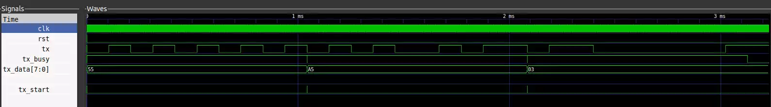
I then compile the uart_tx.v and uart_tx_tb.v file with iverilog as shown in previous blog post and check the timing diagram using GTKWave with following results
UART Receiver Code #
Similarly we can create Reciever block with following state machine:
State machine diagram for UART RX.
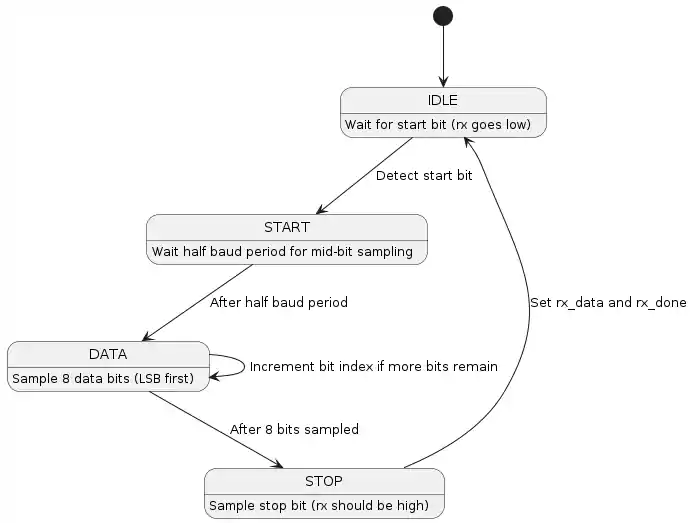
As you can see the Receiver block is bit different from the Transmitter block. There are multiple reasons for this. Firstly, I am using a 50 MHz clock and if you see the line BAUD_COUNTER_MAX = CLOCK_FREQ / BAUD_RATE Our CLOCK_FREQ is not exactly divisible by out BAUD_RATE of 9600. This can cause sampling error in the reciver part. Secondly I made it more robust with double synchronization using rx_sync_0 and rx_synq_1.
module uart_rx #(
    parameter CLOCK_FREQ = 50000000,
    parameter BAUD_RATE  = 9600,
    parameter OVERSAMPLE = 16
)(
    input clk,
    input rst,
    input rx,
    output reg [7:0] rx_data,
    output reg rx_done
);
    localparam integer OVERSAMPLE_MAX = CLOCK_FREQ / (BAUD_RATE * OVERSAMPLE);

    localparam [1:0] IDLE  = 2'b00,
                     START = 2'b01,
                     DATA  = 2'b10,
                     STOP  = 2'b11;

    reg rx_sync_0, rx_sync_1;
    always @(posedge clk) begin
        rx_sync_0 <= rx;
        rx_sync_1 <= rx_sync_0;
    end

    //Registers
    reg [1:0] state;
    reg [15:0] oversample_cnt;
    reg [3:0] sample_cnt;
    reg [3:0] bit_index;
    reg [7:0] rx_shift;

    always @(posedge clk or posedge rst) begin
        if (rst) begin
            state          <= IDLE;
            oversample_cnt <= 0;
            sample_cnt     <= 0;
            bit_index      <= 0;
            rx_shift       <= 0;
            rx_data        <= 0;
            rx_done        <= 0;
        end else begin
            case (state)
                IDLE: begin
                    rx_done <= 0;
                    if (!rx_sync_1) begin
                        state          <= START;
                        oversample_cnt <= 0;
                        sample_cnt     <= 0;
                    end
                end
                START: begin
                    if (oversample_cnt < OVERSAMPLE_MAX - 1) begin
                        oversample_cnt <= oversample_cnt + 1;
                    end else begin
                        oversample_cnt <= 0;
                        sample_cnt     <= sample_cnt + 1;
                        if (sample_cnt == (OVERSAMPLE/2)-1) begin
                            if (!rx_sync_1) begin
                                state     <= DATA;
                                bit_index <= 0;
                            end else begin
                                state <= IDLE;
                            end
                            sample_cnt <= 0;
                        end
                    end
                end
                DATA: begin
                    if (oversample_cnt < OVERSAMPLE_MAX - 1)
                        oversample_cnt <= oversample_cnt + 1;
                    else begin
                        oversample_cnt <= 0;
                        sample_cnt     <= sample_cnt + 1;
                        if (sample_cnt == OVERSAMPLE - 1) begin
                            sample_cnt <= 0;
                            rx_shift[bit_index] <= rx_sync_1;
                            if (bit_index == 7)
                                state <= STOP;
                            else
                                bit_index <= bit_index + 1;
                        end
                    end
                end
                STOP: begin
                    if (oversample_cnt < OVERSAMPLE_MAX - 1)
                        oversample_cnt <= oversample_cnt + 1;
                    else begin
                        oversample_cnt <= 0;
                        sample_cnt     <= sample_cnt + 1;
                        if (sample_cnt == OVERSAMPLE - 1) begin
                            state   <= IDLE;
                            rx_data <= rx_shift;
                            rx_done <= 1;
                        end
                    end
                end
                default: state <= IDLE;
            endcase
        end
    end

endmodule
here is detailed explanation of the code:
The OVERSAMPLE_MAX: This is computed as OVERSAMPLE_MAX = CLOCK_FREQ /(BAUD_RATE * OVERSAMPLE) for us it is OVERSAMPLE_MAX = 50 MHZ /(9600*16)
Before processing the asynchronous rx signal, the code synchronizes it to the clk using a two-stage synchronizer:
reg rx_sync_0, rx_sync_1;
always @(posedge clk) begin
    rx_sync_0 <= rx;
    rx_sync_1 <= rx_sync_0;
end
oversample_cnt counts clock cycles up to OVERSAMPLE_MAX - 1. This counter defines the duration of one oversample period and sample_cnt counts the number of oversample ticks within a bit period. It runs from 0 to OVERSAMPLE - 1. bit_index keeps track of what databit is currently being received from 0 to 7.
IDLE state is state where Receiver waits for transmittion to bigin. I will skip the explaination for this block.
START: begin
    if (oversample_cnt < OVERSAMPLE_MAX - 1) begin
        oversample_cnt <= oversample_cnt + 1;
    end else begin
        oversample_cnt <= 0;
        sample_cnt     <= sample_cnt + 1;
        // When reaching the middle sample of the start bit
        if (sample_cnt == (OVERSAMPLE/2)-1) begin
            // Confirm that the start bit is still low
            if (!rx_sync_1) begin
                state     <= DATA;
                bit_index <= 0;
            end else begin
                state <= IDLE; // False start bit detected
            end
            sample_cnt <= 0;
        end
    end
end
START state is used to validate the reception of start bit. The oversample_cnt is incremented each clock cycle until it completes one oversample period. Once an oversample period is completed, sample_cnt is incremented. When sample_cnt reaches the midpoint of the oversampling window ((OVERSAMPLE/2)-1), the code samples the rx_sync_1 signal and if the signal is still low it confirms a valid start bit and state machine moves to DATA state else it is considered false start ans moved back to IDLE state.
DATA: begin
    if (oversample_cnt < OVERSAMPLE_MAX - 1)
        oversample_cnt <= oversample_cnt + 1;
    else begin
        oversample_cnt <= 0;
        sample_cnt     <= sample_cnt + 1;
        // At the end of the oversample period, consider taking a sample.
        if (sample_cnt == OVERSAMPLE - 1) begin
            sample_cnt <= 0;
            // Optionally, you could implement majority voting over several samples.
            rx_shift[bit_index] <= rx_sync_1;
            if (bit_index == 7)
                state <= STOP;
            else
                bit_index <= bit_index + 1;
        end
    end
end
Similar to the START state the oversample_cnt counts clock cycles for each oversample period.
Once an oversample period completes the sample_cnt is incremented.
When sample_cnt reaches OVERSAMPLE - 1, it indicates that a full bit period has elapsed.
At that moment, the sampled value from rx_sync_1 is stored in the rx_shift register at the position specified by bit_index. If bit_index is 7 state machine transitions to the STOP state
I will leave the STOP bit and compilation and testbench and simulation as homework for the readers of this blog.
Implementing in FPGA #
Now its time to put this in a FPGA and test in real world. I will continue using Altera (Intel) FPGA for now.
We will continue from where we left in my previous blog post link. In this blog we created a basic PLL block that was connected to input clock reference and a GPIO pin at tthe output of the PLL block.
I will remove the output pin as we dont need it anymore and use it as clock input for the uart_rx and uart_tx modules. To create a block diagram from verilog code we can use few simple step first go to File --> New... --> Design Files --> Verilog HDL File to creata a new verilog modules. Then save the abopve code in uart_rx.v and uart_tx.v files. Then start complilation using the button or Ctrl + L button combination in the keyboard. After the compilation is finished, Go to FIles and right click on the uart_tx.v file and Create Symbol Files from current Files:
Do the same for the uart_rx.v and the symbols are now available in main Block Diagram in Project.
For now to test the Reciever and Transmitter block. I will internally connect them or shor circuit them in electrical terms. So the data comming from Receiver is transmitted by Transmitter.
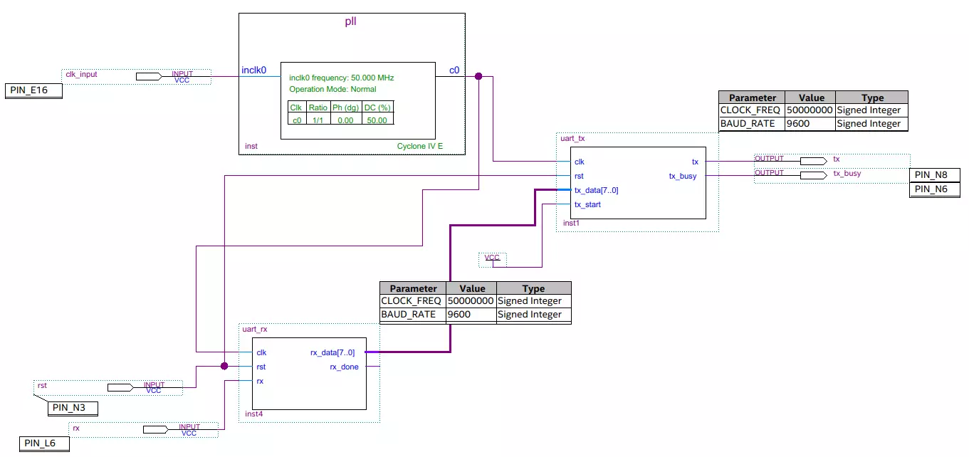
As you can see I have skipped some steps like connecting the GPIO pins to the block as I have already explained it in my previous blog link.
Real World Test #
Now to test it I connected it to a Raspberry Pi (see siagram below) UART Tx pins and created a simple program in Python script to send a counter value over Uart TX which is connected to UART Rx of FPGA board at PIN L6.
import serial
import RPi.GPIO as GPIO
import time

reset = 12
GPIO.setmode(GPIO.BOARD)
GPIO.setup(reset, GPIO.OUT)

GPIO.output(reset, GPIO.HIGH)
time.sleep(1)
GPIO.output(reset, GPIO.LOW)


port = serial.Serial("/dev/serial0", baudrate=9600, timeout=3.0, stopbits=serial.STOPBITS_ONE,bytesize=serial.EIGHTBITS)

counter = 1
while True:
    send_data = counter.to_bytes(1, 'big')
    port.write(send_data)
    counter += 1
    if(counter == 254):
        counter = 1
I have also connected GPIO 18 of Rasperry PI to PIN N3 as reset pin for both uart_rx and uart_tx blocks. This is important as you need to reset and clean all registers.
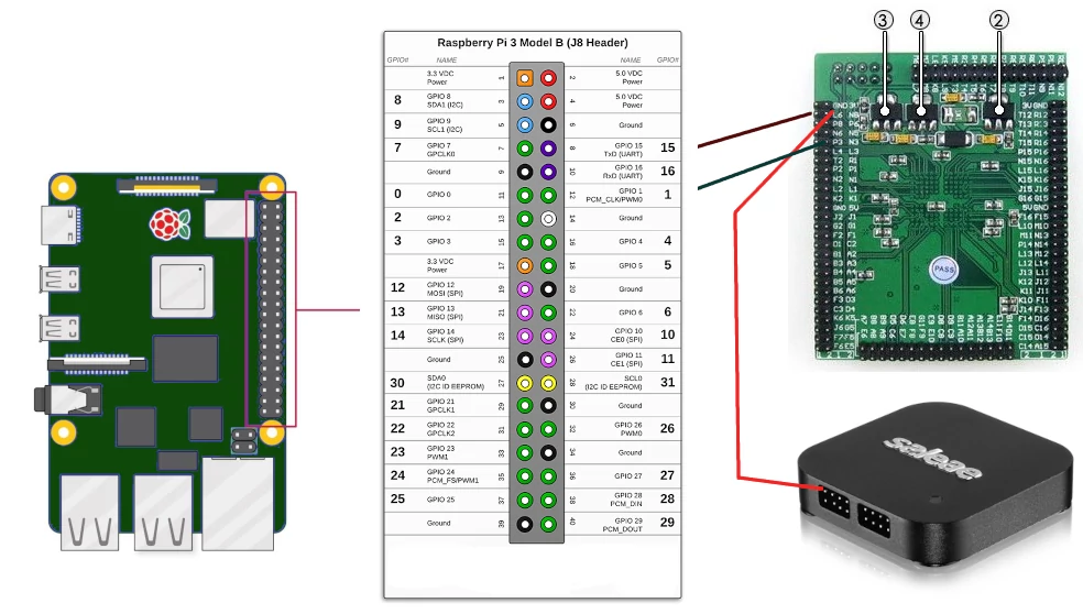
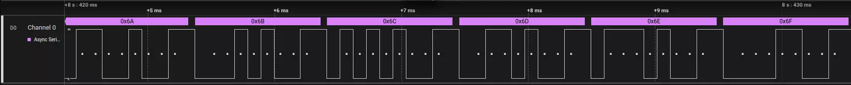
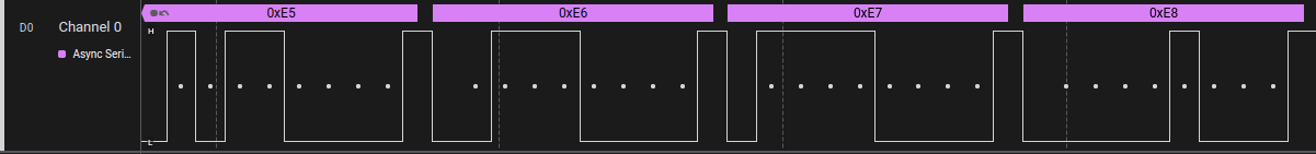
Now I recieve the counter values from the Raspberry Pi Uart Tx and pass it to logic analyser using Uart Tx pin of FPGA.
I get following data:
In future blogs Link I will continue our journey and explore the world of FPGA also we will try other vendors and other modern FPGAs where we dont need to have this interface as the processor is already indife the FPGA as a seperate core.
Tags: #FPGA #Zynq #Xilinx #Altera #Verilog #VHDL #Hardware #Programming #DigitalDesign